Home » Products » Electron Microscopy » FIB-SEM DB550
CIQTEK FIB-SEM DB550
The CIQTEK FIB-SEM DB550 combines high-resolution FE-SEM technology with precise ion beam milling for advanced nanotechnology imaging and materials analysis.
Product Overview
The DB550 FIB-SEM combines advanced Gallium-focused ion beam (FIB) technology with high-resolution imaging capabilities.
It features “super tunnel” electron optics technology and low-aberration, non-magnetic objective design for precise nano-analysis and specimen preparation. With a 0.9nm resolution for imaging and a 3nm milling resolution, it offers powerful capabilities for both imaging and sample modification.
The integrated nanomanipulator and gas injection system enable precise specimen handling and in-situ modification. A retractable scanning transmission electron microscope (STEM) and full software integration streamline operation. The system is ideal for advanced applications such as semiconductor, material science, and nanotechnology.
Features & Benefits
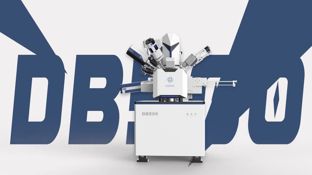
Gallium-focused ion beam for precise nano-analysis and specimen prep.
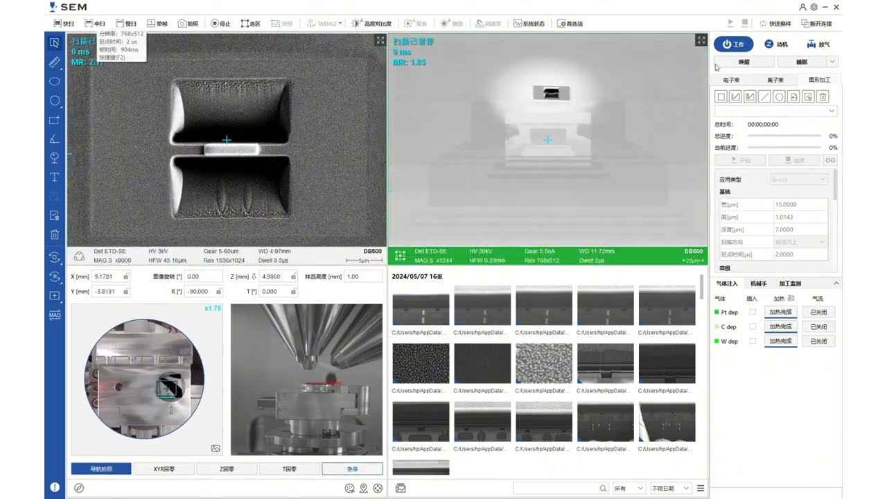
Fully integrated software for seamless co-ordination of imaging and milling.
Super-tunnel electron optics for high-resolution imaging.
Key Features
- Gallium-focused ion beam (FIB) for precise nano-analysis and specimen preparation.
- Super tunnel electron optics technology for high resolution.
- Low aberration, non-magnetic objective design for enhanced accuracy.
- 9nm imaging resolution for detailed imaging at the nanoscale.
- 3nm milling resolution for fine sample modification.
- Integrated nanomanipulator for precise manipulation and specimen positioning.
- Gas injection system for in-situ analysis and specimen handling.
- Water-cooled electromagnetic & electrostatic compound objective lens.
- Full software integration for seamless operation of imaging and FIB.
- Optional plasma cleaner for sample cleaning and preparation.
CIQTEK FIB-SEM DB550 Product Video
Playlist
1:09
6:12
4:34
About the CIQTEK FIB-SEM DB550
The CIQTEK FIB-SEM DB550 represents a significant advancement in electron microscopy, specifically designed to meet the needs of researchers and engineers working in semiconductor failure analysis, nanotechnology imaging, and materials science.
Traditional scanning electron microscopes (SEMs) provide detailed surface imaging, but they often lack the ability to perform precise sample modifications. This is where the FIB-SEM system excels. By integrating a Focused Ion Beam with an electron microscope, users gain the ability to perform high-resolution imaging, cross-section analysis, and precise material modifications, making it an essential tool in cutting-edge research and industry applications.
One of the most significant challenges in semiconductor research and materials science is obtaining clear, high-resolution images of internal structures and the production of TEM cut-out lamella.
The CIQTEK FIB-SEM DB550 solves this by enabling delicate yet effective ion beam milling, allowing scientists to access internal structures and fabricate lamella with optimal results. This capability is essential for semiconductor companies, research institutions, and industries where high quality analysis is critical.
Equipped with advanced FIB-SEM nanofabrication tools, the DB550 enables modifications at the nanoscale, making it a valuable asset in applications such as circuit edit, defect analysis, and micro-device engineering.
For laboratories and industrial users requiring reliable, high-quality results, the CIQTEK FIB-SEM DB550 offers a robust solution. Whether performing electron microscopy with ion beam integration or conducting semiconductor failure analysis, this machine ensures precision and efficiency in every task. Its versatility extends beyond basic imaging, offering advanced nanofabrication capabilities and facilitating research breakthroughs in materials science FIB-SEM applications.
Applications
Semiconductor:
In the semiconductor industry, IC chips may encounter various failures. Various methods are used to analyze the chips to improve reliability. In particular, focused ion beam (FIB) analysis is a reliable analytical technique.
Specimen Characterization / Micro-Nano Fabrication / Cross-section Analysis / TEM Specimen Preparation / Failure Analysis
New Energy Industry:
Observation and analysis of material cross-sections for research and process development.
Morphology Observation / Particle Size Analysis / Cross-section Analysis / Composition and Phase Analysis / Failure Analysis of Lithium-ion Battery Material / TEM Sample Preparation
Ceramic Material:
Material analysis: The FIB-SEM system can perform high-precision micro-nano machining and imaging of ceramic materials, combined with various signal detection modes such as backscattered electrons (BSE), energy-dispersive X-ray spectroscopy (EDX), Electron Backscattered Diffraction Pattern (EBSD), and secondary ion mass spectrometry (SIMS), to study the material in micro to nano-scale with three-dimensional space in depth.
Alloy Material:
To increase the strength, hardness, toughness, etc., of metals, other substances such as ceramics, metals, fibers, etc., are added into the metal using methods such as metallurgy, casting, extrusion, etc., which are called reinforced phases.
TEM specimen prepared by an FIB-SEM is used to observe information such as reinforced phases and boundary atoms through transmitted electron signals. TEM specimens can be used for transmission Kikuchi Diffraction (TKD) analysis, metallographic analysis, compositional analysis, and in-situ testing of alloy cross-section.
Unveiling precision with CIQTEK's FIB-SEM DB550
Product FAQ's
It is ideal for nano-analysis, specimen preparation, material science, and semiconductor research.
It offers 0.9nm imaging resolution, ideal for high-detail nano-scale imaging.
It facilitates in-situ analysis and helps in specimen modification during imaging
The Gallium FIB allows for precise milling and nano-analysis of samples.
Yes, an optional plasma cleaner is available for sample preparation and cleaning.
Contact Us Today
We take great pleasure in assisting you and ensuring you get a prompt response to your questions
Live chat opening hours Mon – Fri 9:15 to 16:30 (UK Time)