
Home » Products » Electron Microscopy » Gentle Ion Beam (GIB)
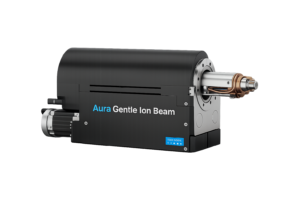
Gentle Ion Beam (GIB)
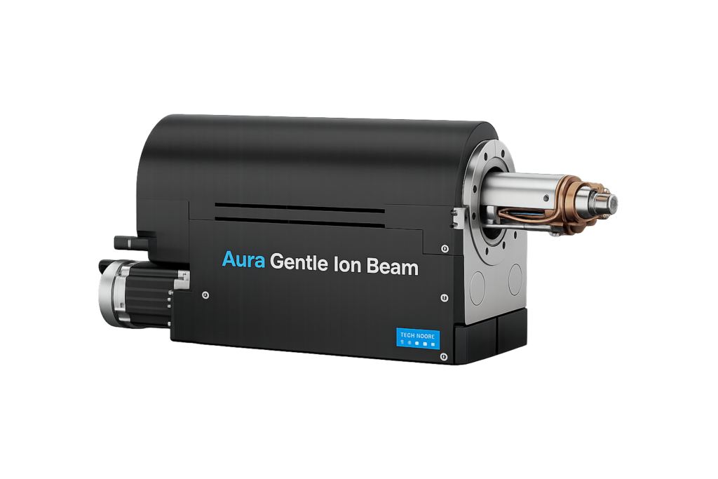
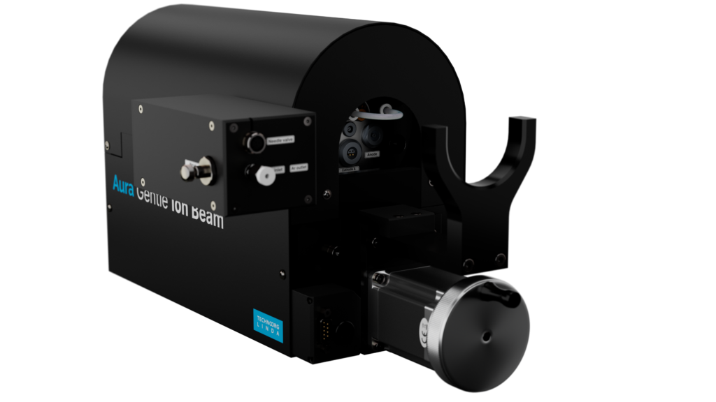
Integrated directly into the electron beam column of your floorstanding SEM, the GIB delivers highly controlled broad ion beam polishing. Achieve artifact-free surface quality for SEM, EBSD, and cross-section analysis – entirely under high vacuum without sample transfer.
Product Overview
Integrated directly into the electron column of floorstanding SEMs, the Gentle Ion Beam (GIB) system eliminates the structural damage, contamination, and deformation caused by conventional mechanical polishing. By utilising precision broad ion beam milling entirely in-situ, it creates exceptionally smooth, artifact-free surfaces without breaking vacuum.
Designed for high-accuracy workflows, the system automates polishing to ensure absolute repeatability while removing operator bias. Whether preparing semiconductor cross-sections, battery materials, metals, or advanced ceramics, the GIB system enables laboratories to seamlessly produce superior, pristine sample surfaces for high-resolution SEM, EBSD, and advanced materials characterization.
Features & Benefits
Protects Sample Integrity
Eliminates amorphization and artifact damage.
Improves Imaging Quality
Creates pristine surfaces for EBSD.
Reduces Preparation Errors
Automated workflows eliminate manual bias.
Supports Difficult Materials
Perfect for fragile semiconductor cross-sections.
Accelerates Laboratory Workflow
In-situ polishing prevents vacuum loss.
Key applications of Gentle Ion Beam (GIB)
Column-Integrated In-Situ Polishing
Operates directly inside the e-beam column of your floorstanding SEM, allowing you to mill, polish, and image under high vacuum without exposing sensitive samples to air.
Broad Ion Beam Technology
Utilises a wide argon ion beam profile to deliver exceptionally uniform, large-area surface preparation and pristine cross-sections.
Artifact-Free Surface Finishing
Eliminates the mechanical stress, deformation, and abrasive contamination inherent to traditional physical grinding and polishing.
Precision Cross-Sectioning
Optimised for semiconductor node evaluation, multi-layered films, and interface analysis, delivering crisp, distortion-free sub-surface boundaries.
Fully Automated Workflows
Features precise, automated recipe processing that minimises operator intervention and ensures highly repeatable sample preparation runs.
Dynamic Beam Parameter Control
Offers fully adjustable voltage and current settings, allowing researchers to optimise milling rates for everything from hard ceramics to beam-sensitive polymers.
Oxidation Prevention
By processing samples entirely within the microscope’s vacuum environment, reactive materials (like lithium battery components) are completely protected from atmospheric degradation.
Advanced Analytical Compatibility
Engineered to provide the ultimate surface flatness required for high-index EBSD mapping, high-resolution SEM imaging, and precision EDS microanalysis.
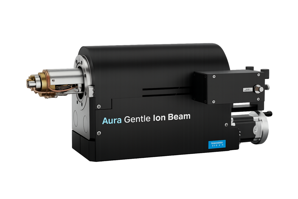
About the Gentle Ion Beam (GIB)
Modern materials analysis increasingly depends on sub-nanometre imaging and characterisation technologies such as high-resolution Scanning Electron Microscopy (SEM), Electron Backscatter Diffraction (EBSD), and Energy Dispersive Spectroscopy (EDS). The ultimate data quality of these advanced analytical techniques depends entirely on one critical bottleneck: sample preparation.
Traditional mechanical polishing systems remain widely used, but they introduce severe subsurface artifacts. Mechanical abrasion inevitably creates deformation layers, smearing, abrasive contamination, and microstructural damage that completely obscure the true nature of the material.
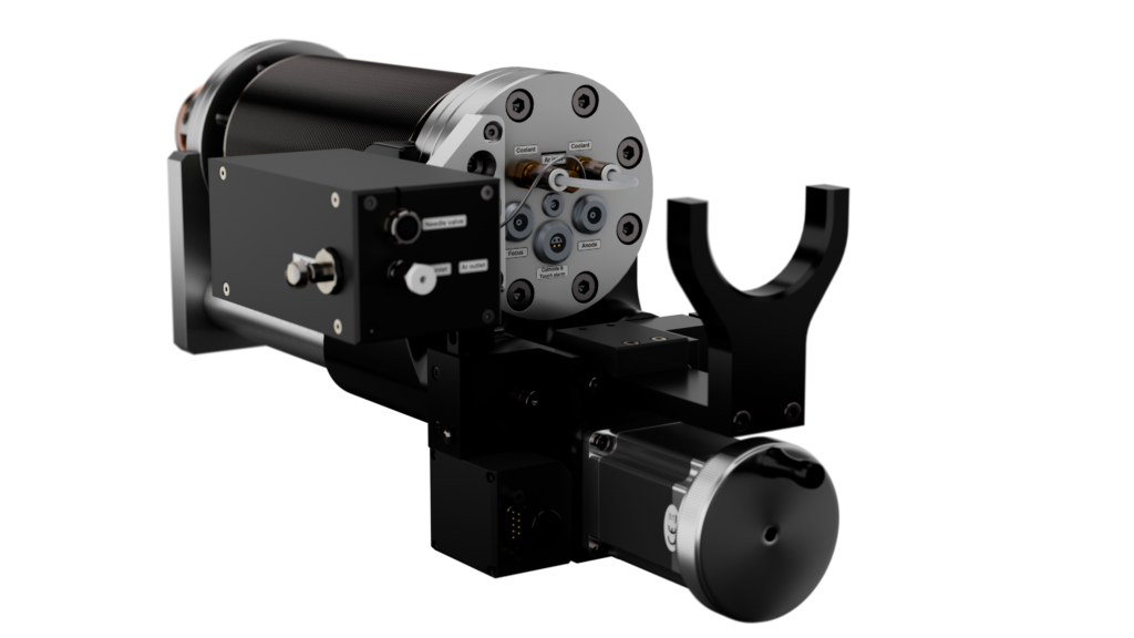
The Gentle Ion Beam (GIB) system eliminates these limitations by introducing highly controlled broad ion beam (BIB) milling technology directly into the electron column of your floorstanding SEM. By using precise, non-contact energetic ion bombardment instead of mechanical abrasion, the GIB system removes material at an atomic level – entirely in-situ
The Power of In-Vacuum, In-Situ Processing
Unlike standalone benchtop ion mills that require transferring sensitive samples through ambient air, the column-integrated GIB system allows researchers to mill, polish, and immediately image specimens under continuous high vacuum. This seamless workflow completely prevents the oxidation, contamination, and atmospheric degradation of reactive materials, unlocking true in-situ material characterisation.
Flawless Preparation for Advanced Materials
Using automated broad ion beam technology, the GIB system removes material uniformly across a large area, preserving pristine sample structure while producing the exceptionally flat, clean surfaces demanded by advanced microscopy:
EBSD and Crystal Orientation Mapping: Crystal orientation indexing requires an entirely deformation-free surface. The GIB eliminates the amorphous top layers that cause pattern degradation, delivering ultra-sharp Kikuchi bands for high-index EBSD mapping.
Semiconductor Failure Analysis:
Engineers require flawless cross-section preparation to inspect sub-micron nodes, multilayer coatings, solder joints, and packaging defects. Mechanical polishing distorts these interfaces; the GIB preserves them with crisp, undeflected boundary lines.
Battery and Energy Storage Research:
Characterising the fragile microstructures of lithium-ion electrodes, separators, and solid-state electrolytes is notoriously difficult. The GIB enables precise cross-sectional polishing without introducing thermal or physical deformation to these highly reactive, beam-sensitive layers.
Operational Consistency and Automation:
The GIB system significantly reduces operator dependency by allowing predefined, automated polishing recipes to be applied consistently across sample batches. This eliminates labour-intensive manual preparation procedures, bypasses user-to-user variability, and guarantees reproducible results.
Maximising Your SEM Investment
For technical procurement teams and laboratory managers, capital equipment evaluation centres on workflow efficiency and analytical throughput. While standalone preparation equipment adds steps, costs, and footprint to the laboratory, the column-integrated GIB system optimises total cost of ownership. It maximises sample survival rates, removes the need for separate vacuum-transfer hardware, and accelerates the time from sample loading to final data acquisition.
As materials become more complex and SEM optics become more advanced, traditional external preparation methods increasingly become the limiting factor. The Gentle Ion Beam column system removes that limitation completely, allowing industrial quality assurance teams, aerospace manufacturers, and elite UK research laboratories to fully unlock the true analytical performance of their floorstanding electron microscopes.
The Gentle Ion Beam (GIB) system delivers in-situ broad ion beam polishing for
floorstanding SEMs, producing pristine, artifact-free surfaces for
high-resolution electron microscopy.
Product FAQ's
While traditional ion beam systems are separate, standalone benchtop instruments, the Gentle Ion Beam (GIB) is a specialized broad ion beam polishing system integrated directly into the electron column of your floorstanding SEM. It uses precise argon ion bombardment to polish sample surfaces at an atomic level without any mechanical contact.
Conventional mechanical polishing introduces subsurface deformation, smearing, and contamination. Standalone ion mills solve this but require transferring samples through ambient air, risking oxidation. The column-integrated GIB system allows you to mill, polish, and image entirely in-situ under continuous high vacuum, keeping reactive samples perfectly pristine.
The GIB is engineered for high-resolution SEM imaging, advanced EBSD crystal orientation mapping, precision EDS microanalysis, semiconductor failure analysis, and cross-sectional material characterisation.
Yes. Because the non-contact polishing occurs entirely inside the microscope’s vacuum environment, the GIB is uniquely suited for fragile, multi-layered, and highly reactive materials (like lithium battery components or thin films) that would degrade if exposed to air or mechanical stress.
Absolutely. It is highly valued for semiconductor defect analysis and packaging evaluation. It produces exceptionally crisp, distortion-free cross-sections of sub-micron nodes, solder joints, and multilayer stacks without the layer smearing caused by mechanical polishing.
EBSD indexing and high-resolution SEM demand a perfectly flat, completely deformation-free surface. The GIB systematically strips away the amorphous artifact layers left behind by previous processing steps, yielding clean surfaces and ultra-sharp Kikuchi bands for precise crystal orientation mapping.
Yes. Lithium-ion battery components, interfaces, and solid-state electrolytes are notorious for their sensitivity to mechanical pressure and atmospheric moisture. The GIB allows battery researchers to cross-section and analyse these fragile layers under continuous vacuum, ensuring true microstructural visualisation.
Contact Us Today
We take great pleasure in assisting you and ensuring you get a prompt response to your questions
Live chat opening hours Mon – Fri 9:15 to 16:30 (UK Time)
Request a Call Back
Please refer to our Privacy statement for information on how SciMed uses your details.
Back to Menu
