
Home » Products » Electron Microscopy » SNE-Alpha Integrated SEM-Raman Spectroscopy System
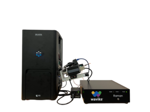
SNE-Alpha Integrated SEM-Raman Spectroscopy System
Correlate high-resolution SEM imaging with Raman molecular analysis to seamlessly map morphology, elemental composition, and chemical identity within a single, compact platform.
Product Overview
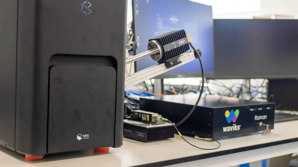
The SNE-Alpha Integrated SEM-Raman System seamlessly combines the compact SEC SNE-Alpha desktop scanning electron microscope with Waviks Vesta Raman technology. This unified platform bridges high-resolution surface imaging with precise molecular fingerprinting and chemical mapping on the exact same sample coordinate. The SNE-Alpha platform delivers an industry-leading resolution down to 5 nm at 30 kV, up to 250,000x magnification, a versatile 1–30 kV accelerating-voltage range, and a precision five-axis motorized stage.
By integrating Raman spectroscopy, researchers unlock critical insights into molecular structure, chemical bonding, and material identity – enabling laboratories to easily differentiate materials with similar morphologies or identical elemental compositions. Depending on your configuration, the system can be further extended with optional EDS and/or EBSD to create the ultimate benchtop characterisation workflow.
Features & Benefits
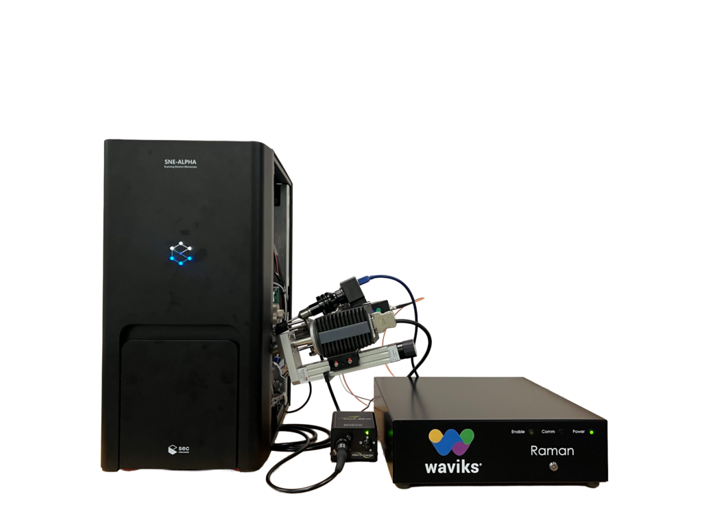
Correlated Analysis
Seamlessly overlay high-resolution SEM morphology with deep Raman molecular insights on a single coordinate.
5 nm Resolution
Resolve intricate nanoscale surface features and morphology at an accelerating voltage of 30 kV.
Molecular Fingerprinting
Definitively identify structural compounds using unique, characteristic Raman vibrational spectra.
Rapid Vacuum Cycle
Accelerate your workflow by reaching full operating vacuum in approximately 90 seconds.
Motorised 5-Axis Navigation
Effortlessly control automated five-axis sample movement for exceptionally accurate target positioning.
Key features & benefits
Correlative SEM-Raman Analysis
Seamlessly overlay high-resolution electron imaging with precise Raman spectra on the exact same coordinate.
High-Resolution Benchtop SEM
Achieve elite performance with a 5 nm resolution at 30 kV and up to 250,000x magnification on a compact platform.
Definitive Molecular Identification
Differentiate structurally similar polymers, minerals, pharmaceuticals, and organic compounds using unique Raman vibrational fingerprints.
Co-Localised Chemical Mapping
Visualise the precise spatial distribution of molecular species and directly correlate chemical data with SEM microstructural morphology.
Accelerated Sample Workflow
Minimise downtime with an ultra-fast 90-second pump-down and a 15-second vent cycle for rapid sample exchanges.
Standard 5-Axis Motorised Stage
Effortlessly navigate complex sample geometries with fully automated, high-precision X, Y, Z, rotation, and tilt positioning.
Standard Dual-Imaging Detectors
Equipped with both Secondary Electron (SE) and Backscattered Electron (BSE) detectors out of the box for comprehensive topography and material contrast.
Expandable Analytical Platform
Future-proof your laboratory by adding optional EDS, EBSD, cathodoluminescence, or EBIC modules as your research demands scale.
Automation-Ready Raman Interface
Features native Ethernet connectivity and a powerful Python SDK via Waviks technology for custom integration and automated analysis routines.
Optimised Laboratory Footprint
Bring floor-model characterisation and deep molecular analysis directly into your space-constrained R&D, QA, or teaching environments.
The SNE-ALPHA by SEC

About the SNE-Alpha Integrated SEM-Raman Spectroscopy System
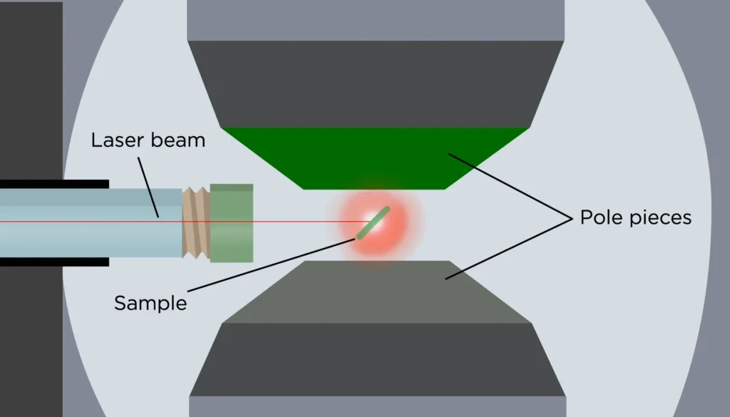
See the feature. Then identify it.
A scanning electron microscope can reveal the shape, texture and position of a microscopic feature with far greater depth of field and resolution than conventional optical microscopy.
That image is often the starting point rather than the final answer. An analyst may see a particle, inclusion, residue, fibre, coating defect or unexpected phase, yet still need to determine what the material is and why it is present. Elemental analysis can add valuable compositional information, but elements alone do not always distinguish compounds, molecular structures or materials that share a similar elemental make-up.
The SNE-Alpha SEM-Raman configuration is designed to close that information gap by combining morphological imaging with Raman molecular fingerprinting.
Correlative SEM and Raman microscopy
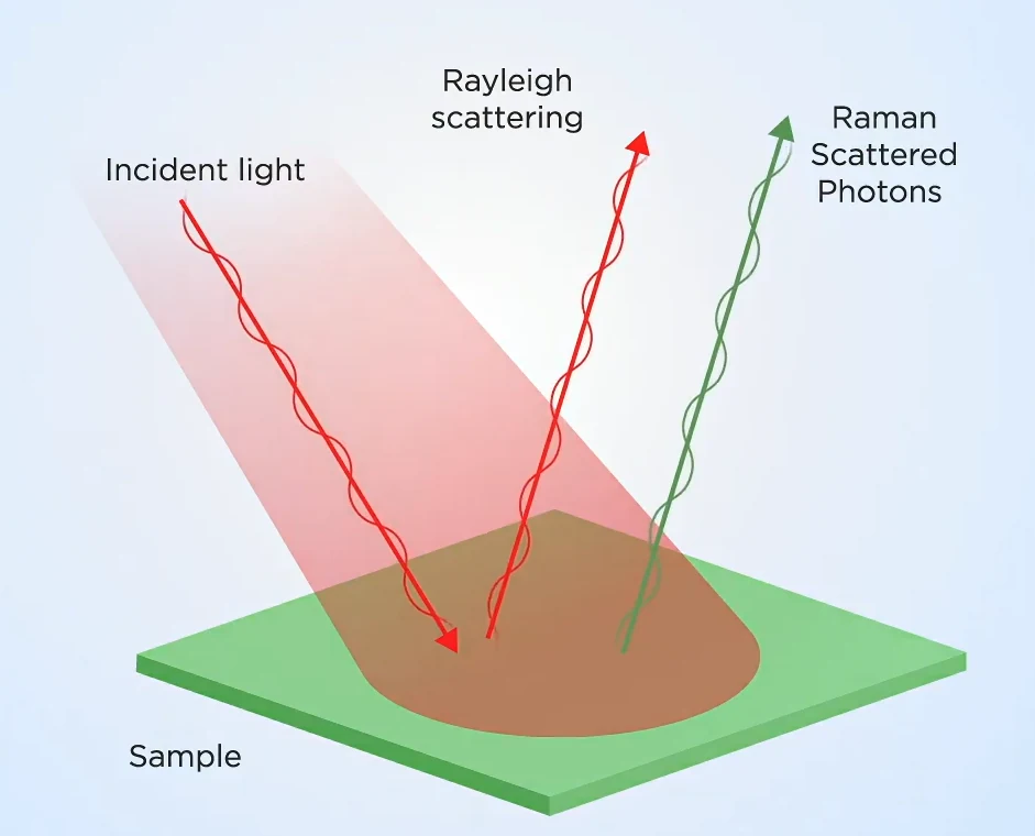
Raman spectroscopy measures the interaction between laser light and molecular vibrations. The resulting spectrum acts as a material fingerprint that can support identification of polymers, minerals, organic compounds, pharmaceutical materials and other Raman-active samples. In a correlative SEM-Raman workflow, the analyst can relate a Raman spectrum to the feature observed in the electron microscope.
The SNE-Alpha desktop SEM platform
At the centre of the system is the SEC SNE-Alpha, a compact scanning electron microscope intended to deliver research-grade imaging on a laboratory bench.
Published specifications include secondary-electron resolution of 5 nm at 30 kV, backscattered-electron resolution of 10 nm at 30 kV and magnification from 20x to 250,000x. The accelerating voltage can be set between 1 and 30 kV in 1 kV steps, giving users flexibility when working with different sample types and imaging requirements.
A pre-centred tungsten hairpin filament provides a familiar and relatively economical electron source. Secondary-electron and backscattered-electron detectors are included, enabling users to switch between topographic and atomic-number contrast.
Designed to fit established sample preparation workflows
The SNRG Block is designed to support common metals digestion procedures, including EPA methods for solid and water samples. Compatible racks, DigiTubes, external temperature sensing accessories and filtration products allow laboratories to build a complete sample preparation workflow around the system.
For UK and Ireland customers, SciMed can advise on the most suitable block size, insert configuration, accessories and consumables for the required sample type, throughput and method.
Faster movement from sample to evidence
The SNE-Alpha is designed for laboratories that need microscopy to fit within an active research, quality or troubleshooting workflow. Pump-down time is approximately 90 seconds and vent time is 15 seconds.
These short cycles can reduce waiting between samples and make routine use more practical. Automated functions include gun alignment, focus, brightness and contrast, helping less-experienced users reach a usable image while allowing specialist operators to retain control over the analytical conditions.
Built-in image stitching supports larger-area views, while three-dimensional surface rendering can help users inspect surface form and roughness.
Controlled positioning and sample navigation
A five-axis motorised stage provides movement in X, Y and Z, plus rotation and tilt. Published travel is 40 mm in X and Y, with 40 mm Z travel, 360-degree rotation and a tilt range from -45 to +90 degrees.
This movement is particularly relevant to a correlated workflow because the sample and region of interest must be positioned accurately for complementary measurements.
Raman performance and integration
The Waviks Vesta Raman system has an f/1.3 high-numerical-aperture spectrometer, spectral resolution below 10 cm-1 and a single-mode laser spot below 10 micrometres.
Multiple excitation wavelengths are supported, including 785 nm, with built-in or externally coupled laser options. The system is modular, permits fibre coupling to an external spectrometer and provides Ethernet communication and a Python software development kit.
An optional Wiley KnowItAll spectral database is listed for material identification.
Extend the analytical workflow
The SNE-Alpha platform includes factory-ready options for complementary analytical techniques. EDS can add elemental composition and distribution, helping identify which elements are present in the region under investigation.
Raman can then help determine the molecular compound or material phase. EBSD may provide crystallographic orientation, phase and texture information for suitable crystalline samples. Cathodoluminescence and electron-beam-induced-current options address specialist semiconductor, mineral and photonic investigations.
Not every application requires every module. SciMed can help users select a configuration based on the samples, questions, throughput and level of correlation required.
Applications across research and industry
The combined platform can support materials science, energy storage, semiconductor inspection, pharmaceuticals, forensics, geoscience, nanomaterials and failure analysis. A battery researcher could compare particle morphology with molecular phase information.
A pharmaceutical scientist could examine particle shape and investigate polymorphic or compositional differences.
A failure-analysis engineer could locate an inclusion, use EDS to establish its elements and apply Raman to refine material identification.
Geoscientists may correlate mineral textures with molecular fingerprints, while semiconductor laboratories can inspect defects and add appropriate analytical modules.
A practical route to in-house capability
For laboratories currently sending samples to a central facility or external provider, a compact SEM-Raman system may reduce turnaround time and keep more of the investigative context within the project team.
The system still requires appropriate sample assessment, preparation, operating procedures and training.
Conductive coating may be needed for some SEM samples, while vacuum compatibility, fluorescence and Raman activity influence whether a sample is suitable for the full workflow.
SciMed can support application review, demonstrations and sample evaluation to help determine whether the proposed configuration answers the customer’s specific analytical questions.
Technical Specifications
"The SNE-Alpha SEM-Raman system combines high-resolution
electron microscopy with molecular identification, helping laboratories
move seamlessly from observing a feature to understanding
its composition and material identity."
Product FAQ's
It integrates a Scanning Electron Microscope (SEM) with a Raman spectrometer into a single, correlative workflow. This allows researchers to instantly link high-resolution surface topography and material structure with precise molecular and chemical identification from the exact same region of interest.
The system is engineered to investigate microscopic particles, material phases, subsurface defects, chemical residues, thin-film coatings, and contaminants. It is ideal for scenarios where electron imaging alone cannot provide enough compositional information for a definitive identification.
Yes. The platform is designed as a Correlative Light and Electron Microscopy (CLEM) system. This integration allows you to acquire high-resolution SEM micrographs and precise Raman molecular spectra from the exact same location on the sample, eliminating the risk of losing your region of interest during sample transfer.
While an SEM provides excellent physical topography and atomic-number contrast, Raman spectroscopy delivers a molecular “fingerprint” based on chemical bonding. This allows you to distinguish between polymers, minerals, pharmaceuticals, organic compounds, and distinct crystalline phases that might otherwise look identical under an electron beam.
Yes. The SNE-Alpha platform is highly modular and supports factory-ready options for multiple complementary techniques. You can combine Energy Dispersive Spectroscopy (EDS) for elemental quantification with Raman spectroscopy for molecular phase analysis, creating a comprehensive analytical suite on a single benchtop.
The SNE-Alpha desktop platform delivers research-grade imaging with a published secondary-electron (SE) resolution of 5 nm at 30 kV, a backscattered-electron (BSE) resolution of 10 nm at 30 kV, and a continuous magnification range spanning from 20x up to 250,000x.
The SNE-Alpha is a highly compact desktop instrument engineered to fit comfortably on a standard laboratory bench. It provides the analytical power and voltage flexibility (1 kV to 30 kV) of conventional microscopy without the heavy space, power, and infrastructure requirements of a traditional floor-standing system.
Sample suitability depends on vacuum compatibility, electrical conductivity, Raman activity, and the material’s sensitivity to laser heating or fluorescence. While some non-conductive samples may require a light conductive coating for optimal SEM imaging, many materials can be analysed directly.
Absolutely. SciMed’s dedicated application team provides comprehensive technical consultations, live instrument demonstrations, and complimentary sample feasibility evaluations. Contact us directly to discuss your specific analytical questions and arrange a review of your target materials.
Contact Us Today
We take great pleasure in assisting you and ensuring you get a prompt response to your questions
Live chat opening hours Mon – Fri 9:15 to 16:30 (UK Time)
Request a Call Back
Please refer to our Privacy statement for information on how SciMed uses your details.
Back to Menu

Frequently Asked Questions
SNE-Alpha SEM-Raman Correlative Microscopy Platform Support