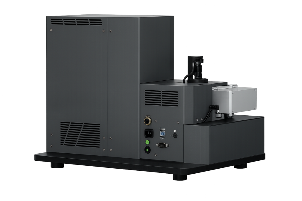
UniMill TEM Sample Preparation System

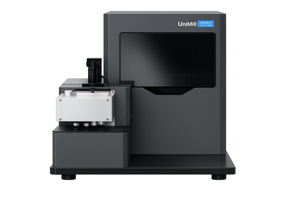
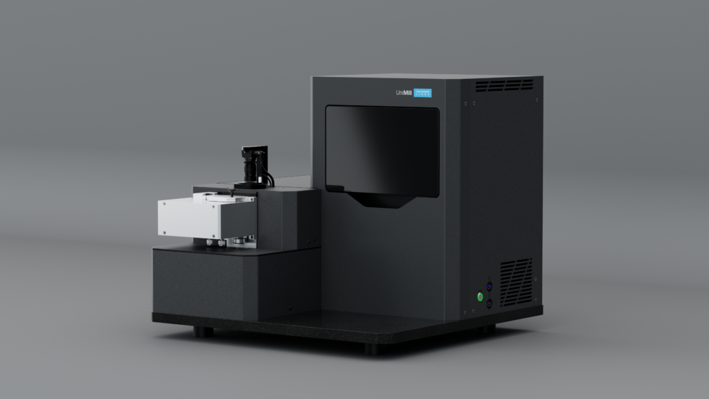
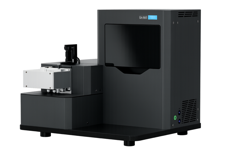
The UniMill is an advanced, automated ion milling system engineered to deliver flawless, artifact-free TEM specimens with absolute reproducibility. Designed for demanding research environments, it automates high-precision site-specific polishing to eliminate the guesswork and accelerate your material analysis workflow.

Product Overview

The UniMill is an advanced, automated ion milling system engineered to deliver flawless, artifact-free TEM specimens with absolute reproducibility. Designed for demanding research environments, it automates high-precision site-specific polishing to eliminate the guesswork and accelerate your material analysis workflow.

Features & Benefits

Automated Operation

Reduces manual intervention and improves consistency

Fine Surface Control

Achieves precise specimen preparation accuracy.

Damage Reduction

Protects sensitive materials during polishing

Flexible Parameters

Optimises preparation for different materials.

High Repeatability

Consistent preparation across every sample.

Fast Preparation

Improves laboratory workflow efficiency.

Broad Compatibility

Suitable across multiple research applications

Precision Engineering

Designed for advanced analytical laboratories
Key applications of UniMill

Automated Ion Beam Control

Fully automated milling processes reduce operator intervention and improve repeatability.

Precision Specimen Thinning

Produces ultra-thin samples required for high-resolution TEM analysis.

Low Energy Polishing

Minimises sample damage during final polishing stages.

Broad Material Compatibility

Suitable for metals, ceramics, semiconductors and composite materials.

Adjustable Milling Parameters

Flexible beam settings for complete process optimisation.

Advanced Sample Rotation

Ensures uniform material removal across specimen surfaces.

Research Grade Precision

Designed for demanding analytical and research applications.

High Workflow Efficiency

Reduces preparation time and increases laboratory productivity.

About the UniMill TEM Sample Preparation System

Transmission electron microscopy remains one of the most powerful analytical techniques available to modern scientists and engineers. However, obtaining high-resolution imaging results depends heavily on one critical stage within the analytical workflow. Sample preparation.

The UniMill TEM Sample Preparation System has been developed to solve one of the most demanding challenges faced by electron microscopy laboratories. Producing ultra-thin, damage-free specimens suitable for advanced microscopy analysis.

Traditional preparation methods often rely heavily on operator skill and can introduce inconsistencies that compromise imaging quality. Mechanical polishing, manual thinning techniques and inconsistent final surface preparation frequently lead to sample artefacts, contamination or structural damage.

The UniMill addresses these challenges through a highly automated ion milling process that delivers exceptional control throughout every preparation stage.

Using advanced broad ion beam technology, the system gradually removes material whilst maintaining tight control over specimen integrity. This allows researchers to prepare specimens that meet the strict thickness requirements needed for transmission electron microscopy analysis.

One of the major advantages of the system is its ability to perform both aggressive bulk material removal and ultra-low energy polishing within a single preparation workflow. High energy ion beam milling enables rapid thinning of harder materials including advanced alloys, ceramics and semiconductor wafers.

Once bulk material removal is complete, low energy polishing allows operators to perform final surface finishing whilst minimising crystal lattice damage and reducing preparation artefacts. This dual-stage capability makes the system highly valuable across a wide range of research environments.

Materials science laboratories use ion milling systems to analyse grain structures, phase boundaries and crystalline defects within advanced alloys and engineered materials.

Semiconductor development facilities rely on high-precision specimen preparation when investigating thin film structures, wafer defects, deposition quality and process failures.

Battery development laboratories use transmission electron microscopy to study lithium-ion degradation, electrode interfaces and material stability within next-generation energy storage systems.

Failure analysis engineers frequently depend on high-quality specimen preparation when investigating structural defects, corrosion pathways and manufacturing inconsistencies.

Academic institutions also benefit significantly from automated preparation systems.

Research teams often work with delicate or highly valuable samples where preparation errors can lead to expensive delays or compromised project outcomes. The UniMill reduces this risk by improving repeatability and reducing operator dependence throughout the preparation process.

Another major advantage lies in laboratory efficiency.

Manual specimen preparation can be time consuming and highly variable depending on operator experience. Automated workflows allow laboratories to standardise preparation procedures whilst increasing sample throughput and reducing preparation bottlenecks.

Another major advantage lies in laboratory efficiency.

Manual specimen preparation can be time consuming and highly variable depending on operator experience. Automated workflows allow laboratories to standardise preparation procedures whilst increasing sample throughput and reducing preparation bottlenecks.

The UniMill automates precision ion milling to produce high-quality, artifact-free
TEM specimens for advanced electron microscopy

Product FAQ's

The UniMill prepares ultra-thin specimens for transmission electron microscopy analysis

Metals, ceramics, semiconductors, composites and advanced research materials.

Yes, the system automates much of the ion milling process

It creates damage-free specimens required for high-resolution imaging

Yes, it is widely suited for semiconductor failure analysis and research.

Yes, low energy polishing helps minimise sample damage

Semiconductors, aerospace, battery development, academia and materials science.


Yes, SciMed offers UK technical sales and application support.

Contact Us Today

We take great pleasure in assisting you and ensuring you get a prompt response to your questions

Live chat opening hours Mon – Fri 9:15 to 16:30 (UK Time)

Request a Call Back

Please refer to our Privacy statement for information on how SciMed uses your details.
Back to Menu